- Home
- All Courses
- Best CMOS & FPGA Design Flow Training in Gurgaon
Best CMOS & FPGA Design Flow Training in Gurgaon & Best CMOS & FPGA Design Flow Training Institute in Gurgaon
 4.9
4.9
out of
5
based on
800user reviews.
Join Best CMOS & FPGA Design Flow Training in Gurgaon, CMOS & FPGA Design Flow Course in Gurgaon, CMOS & FPGA Design Flow Institute in Gurgaon
APTRON delivers an in-depth best CMOS & FPGA Design Flow training in gurgaon. Students having CMOS & FPGA Design Flow certification are able to secure a quick job in an MNC. Participants need to enroll in a best CMOS & FPGA Design Flow training institute in gurgaon to attain the skills involved in the technology. Our core strength is our trainers, who are expert professionals and veteran from the industry. At CMOS & FPGA Design Flow institute in gurgaon, our trainers have developed practical modules combining the syllabus (industry compliance). During the CMOS & FPGA Design Flow course in gurgaon, trainers create realistic situation using simulators and devices.
CMOS & FPGA Design Flow training classes students are asked to take decision concerning to troubleshooting or managing the technology without interrupting the running business operations. Join the best CMOS & FPGA Design Flow training in gurgaon provided by APTRON Gurgaon which equip participants with thorough information, knowledge and experience on the subject.
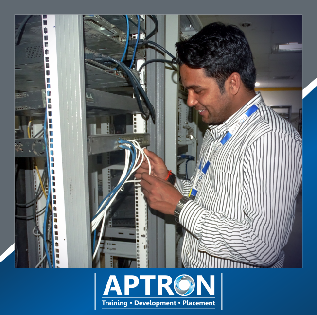
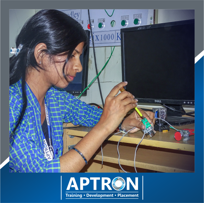
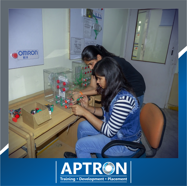
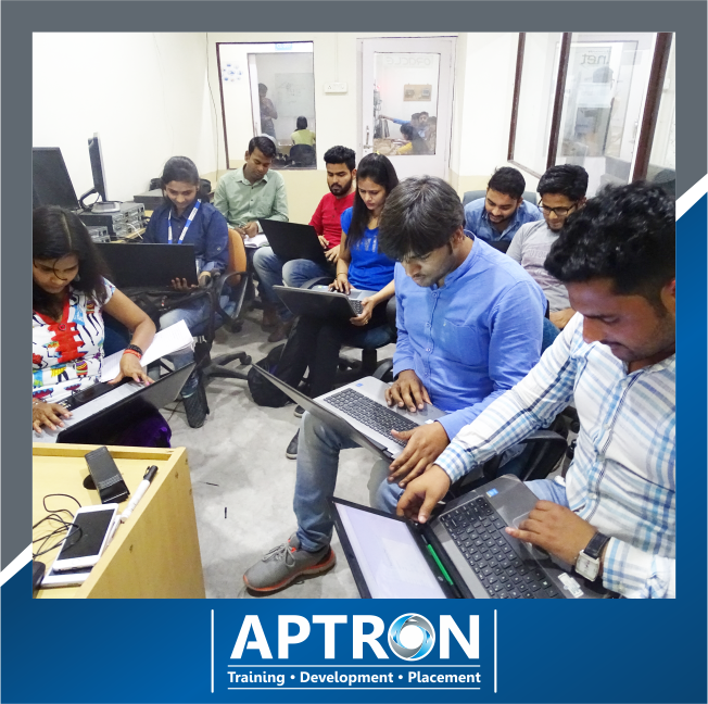
At APTRON, we consider students as our responsibility. Our values inspire us to provide students a comprehensive CMOS & FPGA Design Flow training so that they achieve their career goals confidently. To do that, we have setup a laboratory in accordance to industry standards that comprises of latest devices, applications and softwares. Our whole building is equipped with Wi-Fi facility, latest I.T infrastructure, and smart classroom facilities.
Our responsibility does not end after completion of CMOS & FPGA Design Flow course and certification. We provide CMOS & FPGA Design Flow training course with placement solution to the students. Our placement team schedule placement drives and also conducts interview in different MNCs. Already, we have kept a moderate CMOS & FPGA Design Flow course fee to support students coming from all sections of the society. Further, students find the CMOS & FPGA Design Flow training course duration flexible. CMOS & FPGA Design Flow course time is scheduled according to the student's requirements.
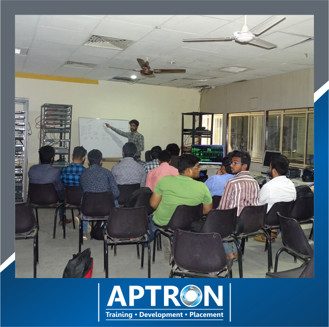
APTRON Gurgaon CMOS & FPGA Design Flow is all about practical and practice; our classes include theory and practical exposure for the students in learning. Join the best CMOS & FPGA Design Flow training in gurgaon provided by APTRON Gurgaon to avail quick CMOS & FPGA Design Flow coaching, moderate course fee, and placement after Ab initio course.
The CMOS & FPGA Design Flow syllabus includes for CMOS & FPGA Design Flow course module on real time projects along with placement assistance. CMOS & FPGA Design Flow topics covered are
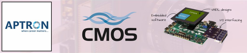
Introduction to VLSI CMOS, Characterization of CMOS Circuits, Layout Representation for CMOS Circuits, Architecture based coding, Back annotation, Gate level simulation, SDF Format,False paths and multi cycle paths
& Many more. Check the duration, course content and syllabus given below.
CMOS & FPGA Design Flow Course Fee and Duration
|
| Track |
Regular Track |
Weekend Track |
Fast Track |
| Course Duration |
45 - 60 Days |
8 Weekends |
5 Days |
| Hours |
2 hours a day |
3 hours a day |
6+ hours a day |
| Training Mode |
Live Classroom |
Live Classroom |
Live Classroom |
Course Content and Syllabus for CMOS & FPGA Design Flow Training in Gurgaon
CMOS & FPGA Design Flow Course Contents
- Introduction to VLSI CMOS
- CMOS Fundamentals and Characterization
- NMOS/PMOS/CMOS Technologies
- Fabrication Principles
- Different Styles of Fabrication for NMOS/PMOS/CMOS
- Design with CMOS Gates
- Characterization of CMOS Circuits
- Scaling Effects
- Sub-Micron Designs
- Parasitic Extraction and Calculations
- Subsystem Design
- Layout Representation for CMOS Circuits
- Design Exercise using CMOS
- Introduction of IC Design
- Different Methodologies for IC Design
- Fabrication Flows and Fundamentals
FPGA Flow
- Re-configurable Devices, FPGA’s/CPLD’s
- Architectures of XILINX, ALTERA Devices
- Designing with FPGAs
- FPGA’s and its Design Flows
- Architecture based coding
- Efficient resource utilization
- Constrains based synthesis
- False paths and multi cycle paths
- UCF file creation
- Timing analysis/Floor Planning
- Place and route/RPM
- Back annotation, Gate level simulation, SDF Format
- DSP on FPGA
- Writing Scripts
- Hands on experience with industry Standard Tools
- ASIC Flow
Project Software Package
Top Reasons to Choose APTRON for CMOS & FPGA Design Flow Training in Gurgaon
- Our CMOS & FPGA Design Flow training in gurgaon adheres to international industry standards.
- We facilitate students with modern I.T infrastructure and learning environment during the CMOS & FPGA Design Flow training in gurgaon.
- Trainers in CMOS & FPGA Design Flow training classes combine the self-developed practice session module with current syllabus.
- Being responsible, we provide students CMOS & FPGA Design Flow course with placement assistance.
- CMOS & FPGA Design Flow training in gurgaon is conducted during weekdays and weekends as per participant's needs.
- Our CMOS & FPGA Design Flow trainers are analysts, researchers, consultants and managers possessing a decade experience in coaching CMOS & FPGA Design Flow course in gurgaon.
- Ultra-modern I.T laboratory equipped with latest infrastructure.
- Our lab is opened 365 days in a year. Students are facilitated with online mentoring during practice sessions.
- CMOS & FPGA Design Flow training classrooms are equipped with projectors, live racks, Wi-Fi, and digital pads.
- We facilitate students with glass-door study room and discussion zone area (meeting room).
- No cost training sessions are conducted on personality development, spoken English, group discussion, and mock interview to sharpen the presentation skills.
- No cost CMOS & FPGA Design Flow training course materials are provided.
- Study materials include books, and soft copies of tutorials in the form of PDFs, sample papers, technical and HR interview questions.
- We also provide hostel facility at Rs.4,500/- a month.
- Our certificates are globally recognized provided after completion of course.
- We facilitate students with Extra Time Slots (E.T.S) for doing unlimited practical at no cost..
- According to the requirements, students can retake the class at no cost.
- To enhance knowledge of the students, the complex technical concepts are imparted through easy coaching.
- We accept master and visa cards (Debit & Credit), also payment mode cash, cheque, and Net Banking available.
APTRON Trainer's Profile for CMOS & FPGA Design Flow Training in Gurgaon
APTRON'S CMOS & FPGA Design Flow Trainers are:
- Our trainers are subject specialist who have mastered on CMOS & FPGA Design Flow technology.
- Our trainers are have received excellence awards for their dedicated CMOS & FPGA Design Flow training and coaching.
- Our trainers are researchers, consultant, and analysts working as an employee in HCL Technologies, Birla-soft, TCS, IBM, Sapient, Agilent Technologies, and so on.
- Our trainers are single, double and triple certified professionals in the subject.
- Our trainers have regular coordination with MNCs HR team on daily basis.
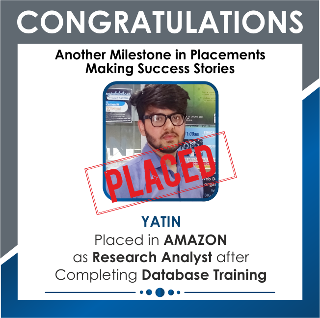
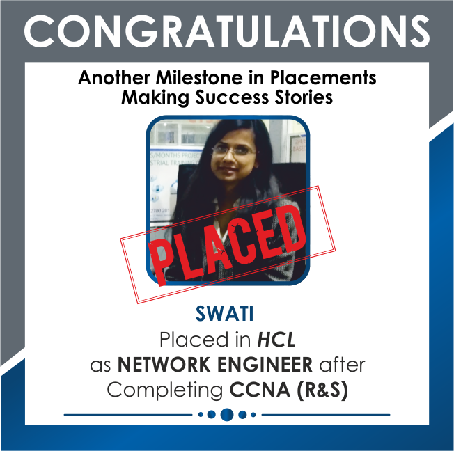
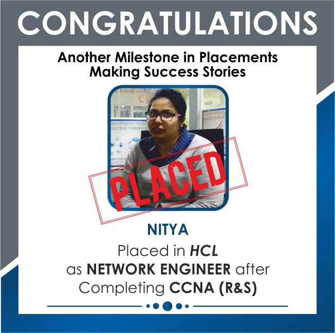
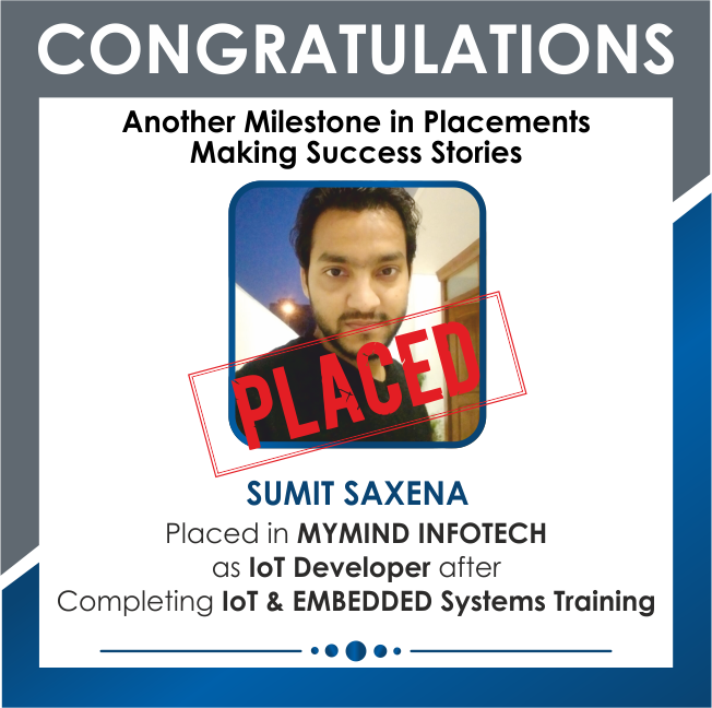
Placement Assistance after CMOS & FPGA Design Flow Training in Gurgaon
APTRON'S Placement Assistance
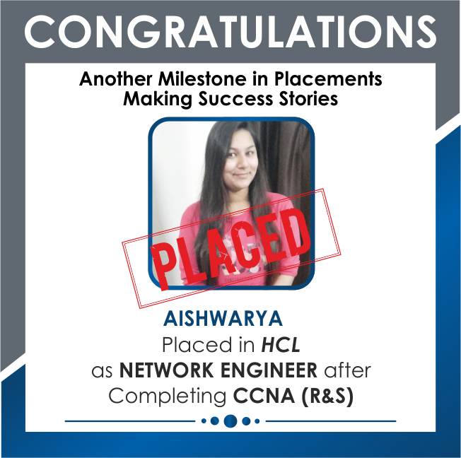
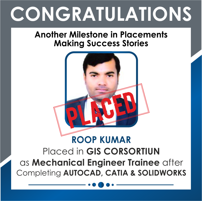
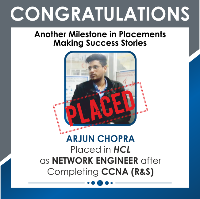
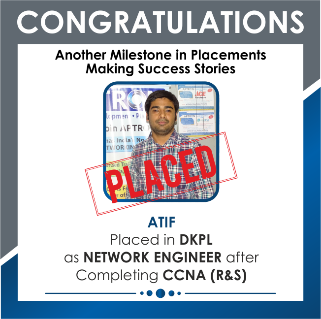
- APTRON's Gurgaon division having successful 96% placement rate.
- APTRON’s CMOS & FPGA Design Flow training centre in Gurgaon assist students in writing their resume meeting the current industry needs.
- APTRON’s CMOS & FPGA Design Flow training institute in Gurgaon sharpens students’ interview skills, provide session on personality development, spoken English, group discussion, mock interview, and presentation.
- APTRON, the best CMOS & FPGA Design Flow training institute in Gurgaon assists students in securing placement in top IT firms such as HCL, TCS, Infosys, Wipro, Accenture, etc., confidently.